sunnuntai 15. joulukuuta 2013

New LO synthesizers

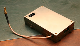
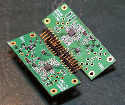
The network analyzer required two local oscillators, easily implementable by phase locking a VCO module. However, having already worked with the ADF4350 chips, it made sense to use them. Well, it made sense to use the modules I already had, but I made new boards for them anyway, simpler and with some mistakes corrected. These are four layer boards as the synthesizer chip loop filter routing needed some shielding not possible with a two layer board.


One of the boards contained a buffer amplifier with a +16dBm output and a mixer, implementing the second downconverter of the analyzer receive path. The mixer covers an RF range of 1.5-4.5GHz, while the synthesizer covers 137MHz-4.4GHz, making the converter generally usable.

The other synthesizer uses the same board, with a difference of a couple of components. The mixer and the amplifier are left out and the RF path routed to a different connector, giving about +6dBm of output to be attenuated and fed to the transmit path mixer.

Both boards also contain a tiny PIC10F206 microcontroller to initialize the synthesizer without needing a separate SPI bus from the system main computer. SPI routing is somewhat difficult, as the computer board only has a few chip select lines. Increasing the number of possible SPI slaves would require a redraw of the interface board with some more thought for the SPI control.


The resulting boards. They will probably require some more supply filtering and perhaps some shielding to improve signal quality. The GPS reference output also seems to require some more work.

Plans for a scalar network analyzer

The signal source project is developing into a scalar network analyzer, and to measure transmission and reflection parameters, a detector is required. After a few diode diode detector designs, which had a low dynamic range in terms of power, a difficultly wide dynamic range in terms of output voltage to be digitized and an unpleasantly nonlinear response, I decided to go heterodyne. Mixing the sweeped signal to a low frequency allows the use of a logarithmic amplifier as a detector, giving a high dynamic range and a log-linear output with easy analog processing. However, at this point the system complexity takes quite a step.


Above is a rough block diagram of the current plan, having already gone through numerous revisions. A number of components were bought for the previous revisions, and then left unnecessary after updates. The microwave relays, couplers, mixers and the power splitter are from eBay. At this point it seems all the finished boards will end up getting redone. Some kind of plans for this have been brewing for 15 years or so, but for the moment the system has reached some level of feasibility and system level maturity. Perhaps something will actually get finished some day...

Though noisy, it makes sense to restrict adjustability to the YIG synthesizer. In order to get a low and constant intermediate frequency for the log amp, the sweeped frequency needs to be mixed with a suitable signal. A 315MHz IF was chosen for the log amp simply because filters for that frequency existed in my component stores. Filtering 315MHz from a signal spanning many GHz would be difficult, so the 4-18GHz YIG output signal is mixed with a constant 3.65GHz signal. A couple of microwave relays select a 2.7GHz low pass filter or a YIG filter with a passband adjustable between 2 and 22GHz, with a bandwidth of around 60MHz. Stretching the output of the YIG synthesizer a bit by replacing the original driver with a self made design, the YIG will go down to 3GHz and up to perhaps 20GHz if needed. This will allow the system to sweep the transmission response of the device under test from 0 to 22GHz. A wideband coupler in series with the output connector also enables the measuring of reflection between 2 and 18GHz.

On the receiver side the YIG synthesizer output is mixed with the signal coming from the DUT (or the reflection path coupler), resulting in an IF of 3.65GHz, which is filtered and then converted to the final 315MHz IF. This requires a separate synthesizer with a frequency of 3.335GHz.

The YIG synthesizers output power varies between +11 and +18dBm, and is further attenuated by the power splitter. With a direct measurement, this variation would need to be corrected by a wideband adjustable attenuator and a feedback loop with a detector and a calibration system. However, in the heterodyne design the variations are reduced quite a bit as the YIG synthesizer output is used only as mixer LO signal, and the transmit side mixer RF input frequency and thus also signal level stay constant. The LO level variation affects the output level very little. The mixer and the filters will have somewhat frequency dependent losses, but I don't yet know whether they are large enough to be bothered with, the total transmission response will be calibrated on the receive side anyway. If some level calibration is required, it is simple to implement by adjusting only the level of the constant frequency synthesizer output feeding the transmit side mixer RF port.

lauantai 7. joulukuuta 2013

Improved frequency reference

At first I was using a 20MHz 2ppm surface mount TCXO as a reference for the synthesizer project, but better precision and phase noise was desired. Having acquired a small 19.2MHz oven controlled oscillator from an old telecom system, I quickly threw together a board for that, with a regulator and a 10-output clock buffer chip. Homemade board and all.


While this worked fine, the local radio amateur electronics recycling team turned up with a high-end oven oscillator board integrated with a 100MHz phase-locked crystal oscillator and a multiplier chain for a 800MHz output. This opened up some possibilities and ideas and warranted the design of a separate complete reference source system. Seems I've lost any unmodified pictures of it separately, it can be seen in later pics.


Ebay provided me with a Jupiter-T GPS module, which has the specialty of having a 10kHz output. There are GPS devices that output 10MHz directly, but the cost was a bit too high. But 10kHz is enough to allow phase locking the oven oscillator to the GPS signal.


As there are no special requirements for the signal speed or phase noise, the PLL can be very simple and have a loop frequency of around 1Hz with a non-critical loop filter. Pictured above is a plug-in board with a 10-output clock buffer, a couple of regulators and a CPLD that contains a clock divider from 10MHz to 10kHz and a phase detector, which together with a simple external RC filter implements the PLL. After an eternity of waiting for the GPS to lock with a weak signal, it showed my spectrum analyzer's internal oven oscillator to have an error of 19Hz at 800MHz.


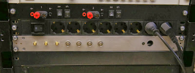
Above pic shows the reference system after integrating the OCXO board and the GPS and PLL boards into a recycled rack enclosure, below a pic of the box integrated into the equipment rack.


Below is the approximate block diagram.


A random mixer


The microwave analyzer project needed a mixer with a low pass filter. The RF/LO band is 4.5-9GHz and the IF 0-2GHz. After feature creep changed the system again, the mixer was left useless.


Classic FR4 casing. Lacks a cover, though.

Phase locking the YIG

While researching the use of the 4-18GHz YIG oscillator, I opened the driver case to make certain which wire goes where. On the oscillator cylinder side, there were two pins without wires connected. The oscillator assembly datasheet mentioned that the device only had a main tuning coil but no FM coil that would allow modulation or more precise frequency control. However, it seems the oscillator itself is a standard part with the FM coil integrated, while the driver block does not connect it to the external connectors FM coil pins. A very lucky find, as this allows phase locking the oscillator!

With a phase lock, the frequency resolution can be improved to a few Hz and frequency precision even better, while the frequency setting speed will improve a lot. As the frequency of a YIG oscillator is set by adjusting the main tuning coil current, it takes up to 10ms before the frequency will have stabilized to the new value. With the smaller and faster FM coil, the output frequency can be locked to the desired frequency in around 100µs, even if the main coil current is still changing (as long as the frequency step is inside the PLL lock range).


After some work, the above PLL block was born. The casing is milled from aluminium. The electronics contains a 4-18GHz prescaler (ADF5002), a fractional-N synthesizer (ADF4157), an active loop filter and a voltage-to-current converter with a differential output to drive the FM coil. With an external 10MHz reference frequency, the system  has a resolution of about 5Hz at 18GHz.

While pretty, the device did not work right away. Not having analyzed the entire system together, I had not included the coil driver and coil itself in the loop coefficients, and the loop was highly unstable. Some considerable rewiring and loop filter recalculations later, the loop stabilized nicely. However, the synthesizer output was rather disappointing. Testing with a Stellex YIG, the phase noise is very nice, hardly measurable with the down conversion setup and spectrum analyzer I used, but connecting the wideband device gave such a noisy signal that it was at least clear that this synthesizer would not be used for a spectrum analyzer preconverter.

YIG oscillators below 8GHz or so are usually bipolar transistor based, but above it GaAs-FETs have traditionally been used, except perhaps in the most modern devices. GaAs devices have far higher 1/f-noise, which translates directly into phase noise, and an ultra wide band device such as the one I'm using will have some compromises made to enable such a bandwidth.


Here's a pic of the modules bolted together.

The synthesizer gains more bandwidth

Prowling through the various surplus shops on eBay, I spotted an old YIG oscillator for which I managed to find a datasheet (which with YIG devices is very rare). YIG (Yttrium-Iron-Garnet) devices are pretty exotic and expensive devices that take advantage of the unusual magnetic properties of the crystal structure of the YIG material. The crystal has a very high Q factor on microwave frequencies and a very narrow resonance point which is very strongly and linearly dependent on the magnetic field. Using an YIG crystal in the feedback loop of an oscillator or as a filter element allows extremely wide tunability with a very good phase noise and with a precise frequency control. The linearity error of frequency vs current throughout the tuning bandwidth may be in the order of 0.1%.

Most modern YIG oscillators contain a permanent magnet to set a base frequency and a magnet coil is used adjust the frequency to either side of the starting point. Common cheap Stellex-made modern YIG oscillators that can be found on eBay have a zero-current frequency around 9GHz and tune +-1GHz. Most YIG devices without a permanent magnet tune by an octave or two.


Above is a picture of two YIG oscillators. The smaller, golden colored is a Stellex-manufactured permanent magnet device with a tuning range of 8-10GHz, while the big and battered device bolted on the heat sink has an internal 12bit DAC and main tuning coil driver and is digitally adjustable for an output of 4-18GHz.

Most YIG devices are designed for a tuning sensitivity of 20MHz/mA, as is this one. It requires +15V for the main supply, -15V for the driver biasing, +5V for the driver logic supply and +28V for a heater that stabilizes the YIG crystal by heating it to around 80°C. I'm not currently using the heater though. So, ignoring the other supplies, the oscillator draws around 100mA from the 15V for the oscillator itself and the current required to set the frequency with the magnet coil. As the tuning range goes from 4GHz to 18GHz, the coil requires a minimum of 200mA for the lowest frequency, going up to 900mA at 18GHz. This means the oscillator will be dissipating around 15W of heat, so without a heat sink it will be running pretty hot.


Here's a snap of the driver block inside the cubical part of the YIG oscillator. I'm not going to open the RF part, it is usually wire bonded and very sensitive. The driver electronics are lacquer coated and pretty robustly built. The device is marked as MIL specified, it probably originates from some obsolete ECM system.


To control the oscillator with the Beagleboard, a control board is required. The above board contains a switch mode regulator that generates the -15V required by the oscillator, an I2C port expander connected to a number of MOSFET's to switch different parts of the system on and off, an I2C bus multiplexer to expand the system control I2C bus, a number of headers to connect to various other modules, and two additional I2C port expanders that feed the 12bit parallel tuning word to the YIG driver DAC. 

Integrated together, the signal generator now had two frequency ranges (but no RF switch between them), covering a total frequency range from 137.5MHz to 18GHz. The YIG device only has a resolution of about 3.4MHz and an accuracy of perhaps 40MHz. 

The system gets computerized

While finishing the signal generator box, it became evident it would be pretty clumsy to use the device for more advanced measurements, even with an external control (it did have a serial port for external control). A proper computer would be needed, capable of controlling the various additional hardware and displaying the data. Creating an user interface using C in a simple embedded environment, including DIY graphics libraries seemed to take much more effort than I had motivation for. I did manage to create control and font maps for a controllerless graphical LCD display, but getting it to draw proper curves and adding various control menus etc. seemed like too much work.

For a while I considered using the ARM processor board with a USB connection to the controlling PC (which on retrospect would probably have been the best choice), but I happened to have a Beagleboard Xm board bought as a toy, which happened to have both SPI and I2C buses I'd need to control various hardware modules. The toy project quickly gathered functionality around it.


In the picture above is the connectivity board I made for the Beagleboard. It has a wide-input switch mode regulator that supplies the 5V needed by the Beagleboard, a number of level shifters to shift the Beagleboard 1.8V logic level I/O ports to 3.3V levels, and an RTC as I had some problems getting the one on the Beagleboard to function properly. Also present are a couple of I2C and SPI headers for external connectivity, and a bus switch to double the number of possible SPI devices. The board has its share of bugs and design errors, but I have not yet made an upgrade.


Here's a pic of the Beagleboard, connectivity board, synthesizer and a quick TCXO board that generates the reference for the synthesizer. The tiny SMD trimmer board in the right edge is a brightness adjustment trimmer for a TFT display panel bought from Chalkboard Electronics, a very nice 10" unpackaged panel with a capacitive touch surface and an adapter board to interface directly to the Beagleboard. 


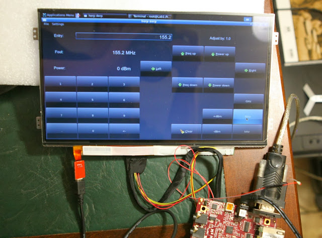
The TFT panel in operation with an early synthesizer GUI. The Beagleboard Xm is running Linux, and learning enough Python and PyGTK to implement a rough GUI took perhaps two weeks of not too intense work in the evenings. The frequency is now adjustable, there are a couple of synthesizer mode settings available though a menu.


At this point I had purchased a 21U 19" rack to house my equipment, and it made sense to integrate the device there. I had no 4U case at hand to attach the screen into, so it is just attached to a front panel, awaiting a separate case or several on the back side of the rack to house the various electronics of the system. The spectrum analyzer is showing the result of a sweep from 137MHz to 3GHz on the synthesizer with a power setting around 10dB below the maximum output. Not very straight line, it would require calibration to level out the response. That has yet to happen...

At this point I was considering a switched chain of multipliers and amplifiers to increase the frequency range, and diode detectors to allow sweeped measurements. It was clear the system would grow in complexity and sophistication, and the only solid part of the design was that it would have to be very modular, with each part adding to the functionality, rather than aiming for some specific totality, or nothing useful would ever get finished...

perjantai 6. joulukuuta 2013

Starting with a microwave synthesizer

So. Electronics has been a hobby for me for two decades or so, and profession for a decade. Being a somewhat active hobbyist, there's a pretty large number of various projects I've worked on. Which is to say, there's not that many projects that have actually made it all the way to getting ready. I'll post some pics and descriptions of some of those older projects if/when I'll bother, mostly I'll be concentrating on the gadgets I'm constructing now.

Lately I've been mostly working on a microwave test system that's been suffering a feature creep of pretty epic proportions. I've done some early drafts of various measurement functionalities as early as 1998, with some not very successful attempts at partial functions once in a while, but the design really started in 2010 when I acquired a couple of ADF4350 chips which allowed the construction of a signal generator with quite little effort.


This was the first module that was finished, it implements a frequency synthesizer with a frequency range of 137.5 MHz to 4.4 GHz with a 5 kHz resolution, and a thermally compensated power control loop with a power adjustment range between about -35 and +5 dBm with a 12 bit DAC control. The synthesizer and DAC are controlled through an SPI bus. Below is a block diagram of the board.


Surprisingly the design worked right away, with just minor adjustments in the PLL loop filter and power control loop gain. The low cost regulators used were however pretty noisy, and switching a lower noise device and some extra supply filtering for significantly improved phase noise left the device rather uglier than pictured above. 

The phase noise is far from awful, but nothing that would compare with a proper test instrument. The power control feedback loop would optimally reduce frequency variation, but of course the detector chip does not have a flat response, resulting in an uncalibrated variation of around 10dB throughout the bandwidth.


The device required some control, of course, and after adding a graphical display, keyboard, an ARM7 card and some power supplies and constructing a pretty slick looking case, the above device was born. However, being a crappy programmer with not that much interest in coding, and with new ideas for the synthesizer drawing my interest elsewhere, the user interface coding slowed and stopped before the device was actually useful. The power reading on the screen is rather more than the device actually outputs, but I never got around to implementing power level settings.